

AD558JN
300 INR
Product Details:
- Input 8-bit digital
- Operating Temperature 0C to +70C
- Response Time Settles to 0.1% in 1 s
- Resolution 8-bit
- Usage Precision D/A conversion in industrial, communications, and instrumentation systems
- Components Integrated resistor, reference, and output buffer
- Power Supply Single supply, 5V
- Click to View more
X
AD558JN Price And Quantity
- 300 INR
- 10 Piece
- 1/2 LSB
- Up to 1 mA at full scale
- Through Hole
- 0V (nominal)
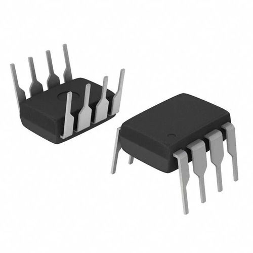
- 8 pins
- Integrated 2.5V reference
- TTL, CMOS
- 1.5 mA (typical)
- 1/2 LSB (typical)
- 2.56V (for 10k reference resistor)
- Microprocessor-based digital-to-analog output, waveform generation, process control
- Yes
- 1/2 LSB (typical)
- 100 pF (max)
- Unipolar
- AD558JN
- PDIP
AD558JN Product Specifications
- 0C to +70C
- Analog voltage output
- +5V (Single Supply)
- 8-bit digital
- Digital to analog conversion, Data acquisition, Instrumentation
- Monolithic DAC (Digital-to-Analog Converter)
- All-in-one DAC solution with reference and output buffer, TTL-compatible, compact DIP-8 packaging
- 5 V DC
- 8-bit
- Integrated Circuit (IC), Monolithic 8-bit DAC
- Settles to 0.1% in 1 s
- Integrated resistor, reference, and output buffer
- Output drive up to 1 mA
- Precision D/A conversion in industrial, communications, and instrumentation systems
- Approx. 5g
- Single supply, 5V
- Black
- Approx. 10.16mm x 7.11mm x 3.3mm
- External DC 5V
- Parallel, TTL-compatible
- Standard DIP-8 package
- 1/2 LSB
- Up to 1 mA at full scale
- Through Hole
- 0V (nominal)
- 8 pins
- Integrated 2.5V reference
- TTL, CMOS
- 1.5 mA (typical)
- 1/2 LSB (typical)
- 2.56V (for 10k reference resistor)
- Microprocessor-based digital-to-analog output, waveform generation, process control
- Yes
- 1/2 LSB (typical)
- 100 pF (max)
- Unipolar
- AD558JN
- PDIP
AD558JN Trade Information
- All India
Product Description
Specification
| Architecture | R-2R |
| Mounting Type | Through Hole |
| Voltage Supply Digital | 4.5 V ~ 16.5 V |
| Supplier Device Package | 16-PDIP |
| Settling Time | 3us |
| Reference Type | Internal |
| Part Status | Obsolete |
| Packaging | Tube |
| Package Case | 16-DIP (0.300", 7.62mm) |
| Output Type | Voltage - Buffered |
| Operating Temperature | 0 deg C ~ 70 deg C |
| Number of DA Converters | 1 |
| Number of Bits | 8 |
| INL or DNL LSB | +-0.5 ( Max ) |
| Differential Output | No |
| Data Interface | Parallel |
| Base Part Number | AD558 |
Highly Integrated Precision DAC
The AD558JN combines an 8-bit DAC, precision 2.5V reference, and output buffer into one device, streamlining your circuit design. This integration reduces the need for external components, ensuring accuracy and consistent output performance. It settles to within 0.1% in just 1 microsecond, ideal for demanding, real-time applications.
Effortless Interface and Compatibility
Designed for seamless connection with TTL and CMOS logic, the AD558JN features a parallel digital input interface for easy integration with mainstream microprocessors. Its standard DIP-8 packaging and through-hole mounting facilitate quick installation, maintenance, and prototyping on various PCB systems.
Reliable Industrial-Grade Performance
Operating over a temperature range of 0C to +70C, the AD558JN meets the rigorous demands of industrial, communication, and instrumentation systems. Its RoHS compliance ensures ecological responsibility, while its robust output drive capability supports loads up to 1 mA at full scale.
FAQs of AD558JN:
Q: How do I use the AD558JN for digital-to-analog conversion in a microprocessor-based system?
A: The AD558JN receives an 8-bit parallel digital input from your microprocessor. Its integrated DAC, reference, and amplifier convert this input to an accurate unipolar analog voltage output, ranging from 0V (zero scale) to 2.56V (full scale with a 10k reference resistor). Simply connect its digital pins to your microprocessors data lines and provide a single 5V supply.Q: What are the typical benefits of using the AD558JN in precision applications?
A: By combining a DAC, precision reference, and buffer in a single package, the AD558JN minimizes external component count, reduces potential error sources, and streamlines circuit design. Its 1/2 LSB INL and DNL, rapid settling time (1s to 0.1%), and TTL/CMOS compatibility make it an optimal solution for precise, fast, and reliable D/A conversion.Q: Where can the AD558JN be implemented effectively?
A: This DAC is well-suited for industrial control systems, waveform generation, digital audio devices, process monitoring, and instrumentation where precise voltage output and fast response are essential. Its through-hole mounting makes it compatible with standard PCBs in laboratory, industrial, and communication settings.Q: What is the process for mounting and connecting the AD558JN?
A: The AD558JN is housed in a standard PDIP-8 package and is designed for through-hole mounting. For connection, solder the device onto any compatible DIP socket or board, wire the digital inputs to your TTL/CMOS-compatible bus, and connect the output to your analog circuit. Supply the device with a regulated external 5V DC power source.Q: How does the built-in reference of the AD558JN benefit my design?
A: The integrated 2.5V reference ensures accurate and stable conversion without requiring an external high-precision reference circuit. This integrated feature not only simplifies board layout and saves component space but also maintains consistent output across temperature and supply variations.Q: What logic levels and interface does the AD558JN support?
A: The AD558JN is fully compatible with both TTL and CMOS logic levels. It uses a parallel digital interface, enabling straightforward connection to most microprocessors and digital controllers operating at standard logic voltages.Tell us about your requirement

Price:
Quantity
Select Unit
- 50
- 100
- 200
- 250
- 500
- 1000+
Additional detail
Mobile number
Email

Other Products in 'Analog Devices IC' category


Contact Details
KK INTERNATIONAL
Mumbai, Maharashtra, India
Mumbai, Maharashtra, India
- Plot No. 305, Rajdeep Apartments, Tara Temple Lane, Near Lamington Road,Mumbai - 400007, Maharashtra, India
- Phone : 08045477473
- Mr Pratik Chouhan (Managing Director)
- Mobile : 08045477473
-
 Send Inquiry
Quick Inquiry

 |
KK INTERNATIONAL
All Rights Reserved.(Terms of Use) Developed and Managed by Infocom Network Private Limited. |
