
AT29C010-70JI Integrated Circuits
90 INR
Product Details:
- Operating Temperature -40C to +85C
- Components High-Density CMOS Flash Circuitry
- Usage Memory Storage in Embedded Systems
- Input TTL-level digital signals
- Output TTL-compatible digital signals
- Power Supply DC
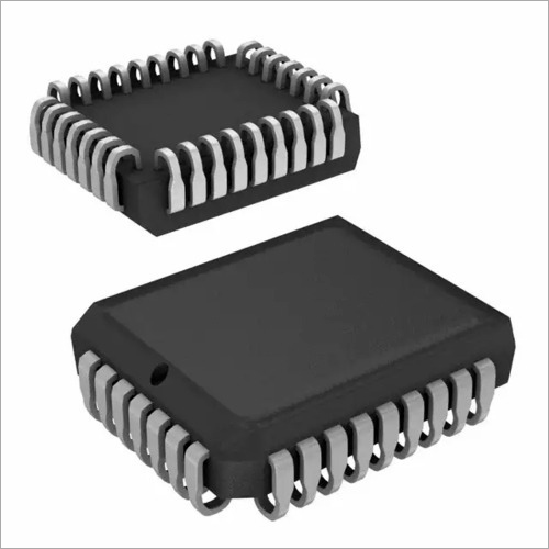
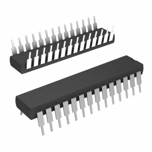
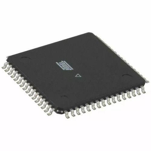
- Interface Parallel (32-pin JEDEC standard)
- Click to View more
X
AT29C010-70JI Integrated Circuits Price And Quantity
- 10 , , Piece
- 90 INR
- 70ns
- 10,000 write/erase cycles minimum
- 10 years minimum
- Software-protected
- Sector (128 x 1024 bytes)
- 5V
- Yes
- 32
- 32-pin SOIC (JEDEC Standard)
AT29C010-70JI Integrated Circuits Product Specifications
- Low Power CMOS, Fast 70ns Access Time, Electrically Erasable and Programmable, Sector or Chip Erase
- Active: 30mA max, Standby: 100A max
- External DC Supply
- 4.5V to 5.5V
- 1-Megabit (128K x 8) CMOS Flash Memory
- Code Storage, Data Storage, Digital Systems
- Black
- Parallel (32-pin JEDEC standard)
- 1 Megabit (128K x 8)
- DC
- Approx. 1g
- High-Density CMOS Flash Circuitry
- Standard JEDEC SOIC package
- TTL-compatible digital signals
- 5V
- TTL-level digital signals
- Memory Storage in Embedded Systems
- Integrated Circuit Flash Memory
- -40C to +85C
- 20.0mm x 7.5mm x 2.35mm (approx)
- Standard 32-pin SOIC
- 70ns
- 10,000 write/erase cycles minimum
- 10 years minimum
- Software-protected
- Sector (128 x 1024 bytes)
- 5V
- Yes
- 32
- 32-pin SOIC (JEDEC Standard)
AT29C010-70JI Integrated Circuits Trade Information
- 3000 , , Piece Per Day
- 2-3 Days
- Yes
- Contact us for information regarding our sample policy
- All India
Product Description
AT29C010-70JI Integrated Circuits are non-volatile flash memories that are greatly admired for assuring superior performance with long service life. They are known to have compact structural configuration hence significantly reduces size of device they are installed in. These ICs are mounted of PCBs by surface mounting technology. AT29C010-70JI Integrated Circuits require voltage supply of 4.5 to 5.5 volts and have write cycle time of about 10ms.
Features:
- Has parallel memory interface
- Excellent quality
- Superior performance
Technical Specification
| Access Time | 70ns |
| Mounting Type | Surface Mount |
| Write Cycle Time Word Page | 10ms |
| Voltage Supply | 4.5 V ~ 5.5 V |
| Technology | Flash |
| Supplier Device Package | 32-PLCC |
| Part Status | Obsolete |
| Packaging | Tube |
| Package Case | 32-LCC (J-Lead) |
| Operating Temperature | -40 deg C ~ 85 deg C (TC) |
| Memory Type | Non-Volatile |
| Memory Size | 1Mb (128K x 8) |
| Memory Interface | Parallel |
| Memory Format | Flash |
| Base Part Number | AT29C010 |
High-Speed Access & Endurance
Experience swift data read and write operations with the AT29C010-70JIs 70ns access time and 10,000 minimum write/erase endurance. This makes it ideal for frequently updated code or data in embedded and digital systems, bolstering reliability even under rigorous use.
Versatile and Durable for Embedded Applications
Benefit from sector-based programming (128 x 1024 bytes) and a proven data retention period of at least 10 years. The device is excellent for memory expansion, code storage, or data logging in automotive, industrial, and consumer equipment, all while maintaining stability over a wide -40C to +85C temperature range.
User-Friendly Integration
Supplied in a standard 32-pin SOIC JEDEC package, the AT29C010-70JI fits easily into existing designs. It is powered by an external DC source (4.5V5.5V) and features TTL-compatible I/O, making it seamless to interface with most microcontrollers and logic systems in embedded settings.
FAQs of AT29C010-70JI Integrated Circuits:
Q: How does the AT29C010-70JI ensure data protection during operation?
A: It utilizes software-controlled write protection, allowing users to safeguard sectors or the entire chip from accidental overwrites. This feature helps maintain data integrity during critical system updates or normal operation.Q: What are the primary applications of the AT29C010-70JI flash memory IC?
A: This component is predominantly used for code and data storage in embedded systems, digital controllers, industrial automation, and applications where quick access and frequent reprogramming are necessary.Q: When should I use the sector erase feature instead of chip erase?
A: Choose sector erase for updating a specific section (128 x 1024 bytes) without affecting the rest of the stored data. Chip erase is suitable when you need to clear or reprogram the entire memory array.Q: Where can the AT29C010-70JI be integrated within an embedded system?
A: This flash memory IC is typically placed on the main board as a non-volatile storage module, interfacing via the parallel data bus supported by the 32-pin JEDEC-standard SOIC package.Q: What is the process for programming and erasing this IC?
A: Programming and erasing are both electrically controlled and performed via standard parallel programming protocols at a supply voltage of 5V, requiring no external high voltage source.Q: How does the device benefit my embedded design?
A: It offers reliable, high-speed memory storage with low power consumption, long data retention, sector-level flexibility, and simple integration, enhancing efficiency and longevity for demanding embedded applications.Tell us about your requirement

Price:
Quantity
Select Unit
- 50
- 100
- 200
- 250
- 500
- 1000+
Additional detail
Mobile number
Email

Other Products in 'Atmel ICS' category


Contact Details
KK INTERNATIONAL
Mumbai, Maharashtra, India
Mumbai, Maharashtra, India
- Plot No. 305, Rajdeep Apartments, Tara Temple Lane, Near Lamington Road,Mumbai - 400007, Maharashtra, India
- Phone : 08045477473
- Mr Pratik Chouhan (Managing Director)
- Mobile : 08045477473
-
 Send Inquiry
Quick Inquiry

 |
KK INTERNATIONAL
All Rights Reserved.(Terms of Use) Developed and Managed by Infocom Network Private Limited. |
