
AT89C51RD2UM
150 INR
Product Details:
- Usage Embedded System Applications
- Components AT89C51RD2UM Chip
- Processor Speed 40 MHz
- Output Digital
- Power Source External DC supply
- Interface UART, SPI, I2C
- Operating Temperature -40C to +85C
- Click to View more
X
AT89C51RD2UM Price And Quantity
- 150.00 - 250.00 INR
- 10 Piece
- 150 INR
- 2
- 8-bit
- 1792 Bytes (1.75 KB)
- Crystal
- 32
- Supported
- Yes
- No EEPROM
- 100,000 Write/Erase Cycles
- 5 V
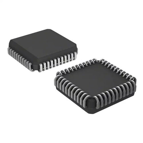
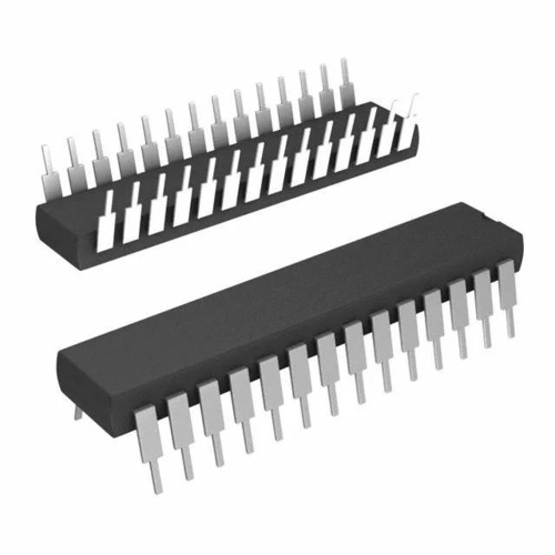
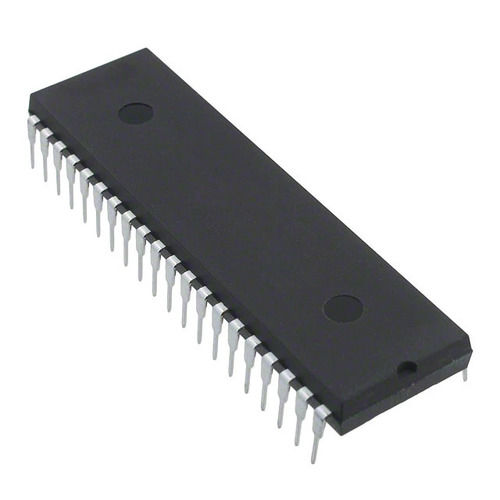
- DIP-40, PLCC-44 and TQFP-44 Available
- Supported by Popular 8051 Debuggers & Programmers
- Yes
- 3 x 16-bit
- Supported
- 8051 Compatible
- 10 Years at 85°C
AT89C51RD2UM Product Specifications
- Standard IC Package
- 40 MHz
- Microcontroller IC
- AT89C51RD2UM Chip
- Consumer Electronics, Industrial Automation, Embedded Systems
- 40 MHz Max
- 25 mA (Maximum) typ.
- Embedded System Applications
- 64 KB Flash Memory
- 4.0 V to 5.5 V
- Digital
- Black
- In-System Programming, Enhanced CPU, 2 UARTs, Up to 64 KB ISP Flash
- DC
- -40C to +85C
- Approx. 52 mm x 15 mm x 5 mm
- UART, SPI, I2C
- 5 V
- Microcontroller Unit
- Digital
- External DC supply
- 40 Pin DIP
- Approximately 3 grams
- 2
- 8-bit
- 1792 Bytes (1.75 KB)
- Crystal
- 32
- Supported
- Yes
- No EEPROM
- 100,000 Write/Erase Cycles
- 5 V
- DIP-40, PLCC-44 and TQFP-44 Available
- Supported by Popular 8051 Debuggers & Programmers
- Yes
- 3 x 16-bit
- Supported
- 8051 Compatible
- 10 Years at 85°C
AT89C51RD2UM Trade Information
- All India
Product Description
Specification
| ADC Resolution | No ADC |
| Length | 16.7 mm |
| Width | 16.7 mm |
| Unit Weight | 0.084185 oz |
| Supply Voltage Min | 2.7 V |
| Supply Voltage Max | 5.5 V |
| Subcategory | Microcontrollers - MCU |
| Program Memory Type | Flash |
| Program Memory Size | 64 kB |
| Processor Series | AT89x |
| Packaging | Tube |
| Package Case | PLCC-44 |
| Operating Supply Voltage | 2.7 V to 5.5 V |
| Number of Timers Counters | 3 Timer |
| Number of IOs | 32 I/O |
| Mounting Style | SMD/SMT |
| Minimum Operating Temperature | - 40 C |
| Maximum Operating Temperature | + 85 C |
| Maximum Clock Frequency | 60 MHz |
| Interface Type | SPI, UART |
| Height | 3.48 mm |
| Data RAM Size | 2 kB |
| Data Bus Width | 8 Bit |
Versatile Architecture for Embedded Systems
The AT89C51RD2UM microcontroller harnesses an 8051-compatible architecture, ensuring seamless integration into established development environments. Its 8-bit data width promotes efficient data handling, while on-chip debug features and system-level interfaces make it a practical choice for rapid prototyping in embedded solutions ranging from consumer electronics to industrial controls.
Robust Memory and Data Retention
With 64 KB In-System Programmable (ISP) Flash and 1792 Bytes of RAM, the AT89C51RD2UM provides ample space for code and data storage. The flash memory supports up to 100,000 write/erase cycles and guarantees data retention for at least 10 years at temperatures up to 85C, ensuring reliability in long-term and critical applications.
Comprehensive Connectivity and I/O
Equipped with 32 I/O pins, 2 PWM channels, and communication interfaces including UART, SPI, and I2C, the AT89C51RD2UM offers flexible and extensive I/O options. Its external memory interface further broadens its applications, allowing for expansion in complex embedded projects.
FAQs of AT89C51RD2UM:
Q: How is the AT89C51RD2UM programmed and debugged?
A: The AT89C51RD2UM supports in-system programming (ISP) and on-chip debug, enabling you to program and debug the microcontroller directly on the target board with popular 8051-compatible debuggers and programmers. This facilitates efficient development and troubleshooting without removing the chip from its circuit.Q: What are the primary usage applications for the AT89C51RD2UM microcontroller?
A: This microcontroller is ideal for use in embedded systems, including consumer electronic devices, industrial automation solutions, and other applications requiring reliable digital control and robust memory. Its versatility also makes it suitable for prototyping and educational purposes.Q: When should I choose the AT89C51RD2UM for my project over other microcontrollers?
A: Choose the AT89C51RD2UM when your project requires an 8051-compatible microcontroller with substantial Flash and RAM, a wide input voltage range, hardware timers, multiple communication interfaces (UART, SPI, I2C), and robust data retention. It is particularly advantageous for applications needing long-term reliability and frequent reprogramming.Q: Where can I source the AT89C51RD2UM microcontroller in India?
A: You can purchase the AT89C51RD2UM from electronic component distributors, manufacturers, importers, suppliers, traders, and wholesalers throughout India. Both online and offline distribution channels are available for procurement.Q: What benefits does the AT89C51RD2UM offer in industrial environments?
A: In industrial settings, the AT89C51RD2UM delivers high processing speed (up to 40 MHz), wide operating temperature range (-40C to +85C), and 100,000 flash write/erase endurance. Its watchdog timer, multiple I/O, and robust connectivity interfaces ensure reliability and consistent system performance.Q: How does the external memory interface expand the capabilities of the AT89C51RD2UM?
A: The external memory interface allows users to connect additional memory or peripheral devices, enabling the development of more complex embedded systems beyond the built-in resources, thus supporting applications requiring greater data storage or additional functionalities.Q: What is the process for integrating the AT89C51RD2UM into a new embedded system design?
A: Integration involves selecting a suitable package (DIP-40, PLCC-44, or TQFP-44), designing the PCB to accommodate 32 I/O pins and required interfaces, configuring the oscillator, connecting the power supply (4.0 V to 5.5 V DC), and using a supported programmer to load the application firmware via ISP.Tell us about your requirement

Price:
Quantity
Select Unit
- 50
- 100
- 200
- 250
- 500
- 1000+
Additional detail
Mobile number
Email

Other Products in 'Atmel ICS' category


Contact Details
KK INTERNATIONAL
Mumbai, Maharashtra, India
Mumbai, Maharashtra, India
- Plot No. 305, Rajdeep Apartments, Tara Temple Lane, Near Lamington Road,Mumbai - 400007, Maharashtra, India
- Phone : 08045477473
- Mr Pratik Chouhan (Managing Director)
- Mobile : 08045477473
-
 Send Inquiry
Quick Inquiry

 |
KK INTERNATIONAL
All Rights Reserved.(Terms of Use) Developed and Managed by Infocom Network Private Limited. |
