
OP491GP
230 INR
Product Details:
- Interface Through Hole (DIP/SIP Package)
- Operating Temperature -40C to +85C
- Components Semiconductor Die, Metal Pins, Plastic Encapsulation
- Input 4 Independent Op-Amps
- Response Time Slew Rate: 0.3 V/s
- Usage General purpose amplification, signal conditioning
- Power Supply Dual or Single Supply
- Click to View more
X
OP491GP Price And Quantity
- 230 INR
- 10 Piece
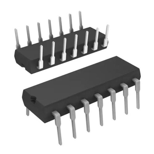
- PDIP, 9-Pin SIP
- 9
- 0V to (V+ - 1.5V)
- Max 2 mV
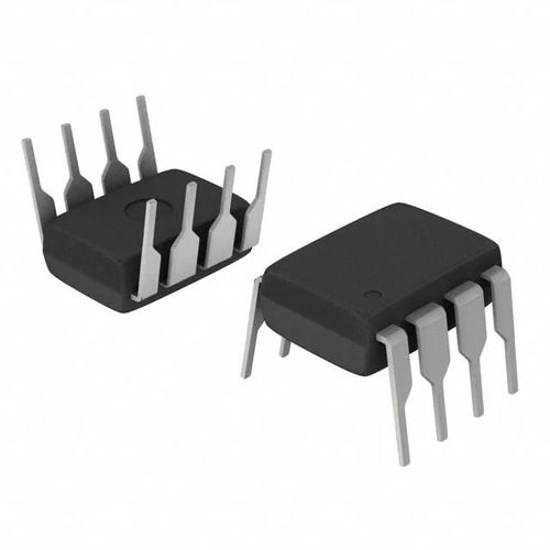
- Through Hole
- Yes
- Quad Single-Supply Op-Amp
- 80 dB (min)
OP491GP Product Specifications
- 2V to 18V
- Operational Amplifier Signal Outputs
- Quad Operational Amplifier
- Integrated Circuit (IC)
- Approx 10.16mm x 3.56mm x 2.92mm
- Instrumentation, Sensor Interfaces, Signal Buffering, Active Filters
- 4 Independent Op-Amps
- Input Bias Current: 7nA (max)
- Quad (4) Amplifier Channels
- Approximately 0.4g (9-Pin Package)
- Low offset voltage, low bias current, low power consumption, high common-mode rejection ratio
- Standard (Integrated Circuit Black Package)
- Unity-Gain Bandwidth: 600 kHz
- 9-Pin SIP, Standard IC Size
- General purpose amplification, signal conditioning
- Slew Rate: 0.3 V/s
- Through Hole (DIP/SIP Package)
- Dual or Single Supply
- -40C to +85C
- Standard IC Thickness
- +3V to +36V (Single Supply) / 1.5V to 18V (Dual Supply)
- Semiconductor Die, Metal Pins, Plastic Encapsulation
- Powered via Supply Pins (V+, V-)
- PDIP, 9-Pin SIP
- 9
- 0V to (V+ - 1.5V)
- Max 2 mV
- Through Hole
- Yes
- Quad Single-Supply Op-Amp
- 80 dB (min)
OP491GP Trade Information
- All India
Product Description
Specification
| Common Mode Rejection Ratio | 70 dB |
| Number of Pins | 14 |
| Length | 19.05 mm |
| Width | 6.35 mm |
| Voltage Gain | 96.9 dB |
| Unity Gain Bandwidth Product | 3 MHz |
| Slew Rate | 0.4 V/us |
| Power Supply Rejection Ratio PSRR | 80 dB |
| Operating Supply Voltage | 9 V |
| Number of Elements | 4 |
| Mount | Through Hole |
| Min Supply Voltage | 2.7 V |
| Min Operating Temperature | -40 deg C |
| Min Dual Supply Voltage | 1.35V |
| Max Supply Voltage | 12V |
| Max Supply Current | 1.6 mA |
| Max Operating Temperature | 125 deg C |
| Max Dual Supply Voltage | 6V |
| Input Offset Voltage Vos | 700 uV |
| Input Bias Current | 65 nA |
| Height | 3.3 mm |
| Gain Bandwidth Product | 3 MHz |
| Dual Supply Voltage | 5V |
High Performance Quad Op-Amp
The OP491GP is engineered for high accuracy with a low input offset voltage of up to 2 mV and a minimum common-mode rejection ratio of 80 dB. This ensures stable and precise signal amplification where noise or voltage shift could impact sensitive measurements, making it ideal for demanding analytical tasks.
Flexible for Multiple Applications
With four integrated amplifiers in a single IC, the OP491GP is versatile for tasks like signal conditioning, instrumentation, sensor interfaces, active filters, and buffering. Its compatibility with both single and dual supply options allows it to adapt to various circuits, providing efficient signal handling in industrial and laboratory settings.
Reliable and Convenient Design
Housed in a standard 9-Pin SIP or PDIP through-hole package, the OP491GP supports straightforward installation on PCBs. Its robust operational range (-40C to +85C) and low power consumption make it suitable for continuous use in diverse environments, and its RoHS compliance ensures safe handling and component sourcing.
FAQs of OP491GP:
Q: How does the OP491GP ensure accurate signal amplification in instrumentation applications?
A: The OP491GP features a low input offset voltage (max 2 mV) and a high common-mode rejection ratio (min 80 dB), minimizing error and interference, which is critical for precise signal amplification in instrumentation and sensor systems.Q: What voltage supplies are compatible with the OP491GP operational amplifier?
A: The OP491GP supports both single supply voltages (+3V to +36V) and dual supply voltages (1.5V to 18V), providing flexibility for integration into various analog and mixed-signal designs.Q: When is the OP491GP recommended for use in active filter circuits?
A: The OP491GP is ideal for active filter circuits due to its unity-gain bandwidth of 600 kHz and reliable slew rate of 0.3 V/s, enabling it to process AC signals efficiently within its frequency range.Q: Where can the OP491GP be mounted in electronic systems?
A: The OP491GP is supplied in a 9-Pin SIP or PDIP through-hole package, making it suitable for mounting on standard through-hole printed circuit boards commonly used in development, prototyping, and production systems.Q: What is the process for integrating the OP491GP into a sensor interface application?
A: To integrate the OP491GP in a sensor interface, designers can connect sensor outputs to any of the four independent op-amp inputs, utilizing single or dual supply configurations, and route amplified outputs to downstream circuitry for further processing or digitization.Q: How does RoHS compliance benefit users of the OP491GP?
A: RoHS compliance ensures the OP491GP is free from hazardous substances like lead, making it safe for use in consumer, industrial, and medical electronics within global markets that require environmental safety standards.Q: What are the advantages of using the OP491GP for general-purpose signal conditioning?
A: Benefits include multiple amplification channels in a compact package, low input bias current (max 7 nA), efficient voltage swing, minimal power consumption, and robust operation across a wide temperature range, optimizing signal integrity and reliability.Tell us about your requirement

Price:
Quantity
Select Unit
- 50
- 100
- 200
- 250
- 500
- 1000+
Additional detail
Mobile number
Email

Other Products in 'Analog Devices IC' category


Contact Details
KK INTERNATIONAL
Mumbai, Maharashtra, India
Mumbai, Maharashtra, India
- Plot No. 305, Rajdeep Apartments, Tara Temple Lane, Near Lamington Road,Mumbai - 400007, Maharashtra, India
- Phone : 08045477473
- Mr Pratik Chouhan (Managing Director)
- Mobile : 08045477473
-
 Send Inquiry
Quick Inquiry

 |
KK INTERNATIONAL
All Rights Reserved.(Terms of Use) Developed and Managed by Infocom Network Private Limited. |
